
Updated April 24, 2023
In this application note we present details of making measurements of the gain and phase of a linear voltage regulator. We employ an injection transformer to inject a small signal into the feedback loop and observe phase margins of two different load capacitors. This procedure is compatible with Moku:Go, Moku:Lab, and Moku:Pro.

Frequency Response Analyzer
The Moku:Lab Frequency Response Analyzer (FRA) drives a swept sine wave on the Moku outputs and simultaneously measures the received signal amplitude (or power) and phase on the Moku inputs. This can be used to measure the transfer function of a system or device under test and thus create a plot of amplitude and phase vs frequency, commonly referred to as a Bode plot. In this application, we inject the swept sine into the feedback loop of a linear voltage regulator and assess the phase margin of the control loop.
A linear voltage regulator design incorporates a feedback loop to maintain voltage regulation. In order to measure the control loop response, we need to inject a disturbance signal. This is usually accomplished by inserting a small value resistor into the control loop. This is referred to as the injection resistor (Rinj), across which we can then inject the test or disturbance signal.
Moku:Lab, in common with most test equipment, has grounded inputs and outputs. The Rinj does not have a ground connection and thus we need a way to isolate the Moku output. This is done by the use of a transformer and in our application, we use an injection transformer from Picotest (model J2101A).
Test device and setup
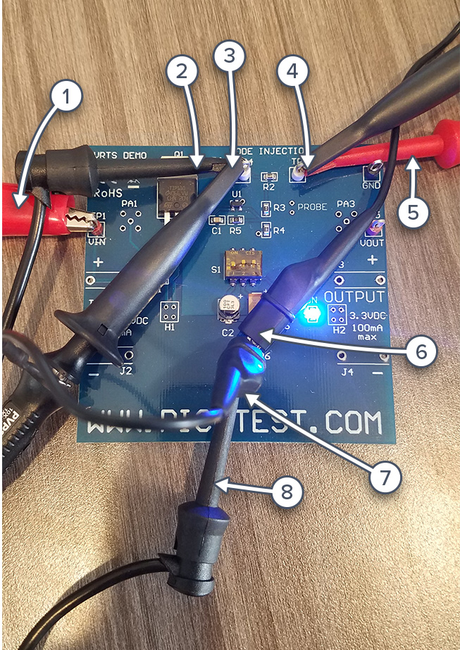
The device we have chosen to test is a Picotest VRTS 1.5 board, figure 1 is the schematic. This board implements a shunt regulator (U1), controlling a BJT (Q1). The input voltage range is 7-10v and the output is preset by resistor pair R3 & R4 to be 3.3v. This VRTS board provides suitable breakout points for probing, also the injection resistor R2 is in the feedback loop with a value with 4.99 ohms. Test points TP3 and TP4 provide connections for both the injector transformer and the measurement probes. S1 provides options to select output capacitors C2 or C3, both 100uF. C2 is an aluminum electrolytic while C3 is a tantalum capacitor. Additionally, R6 may be selected to provide a 25mA load. The LED provides an indication that the VRTS is powered and operating.
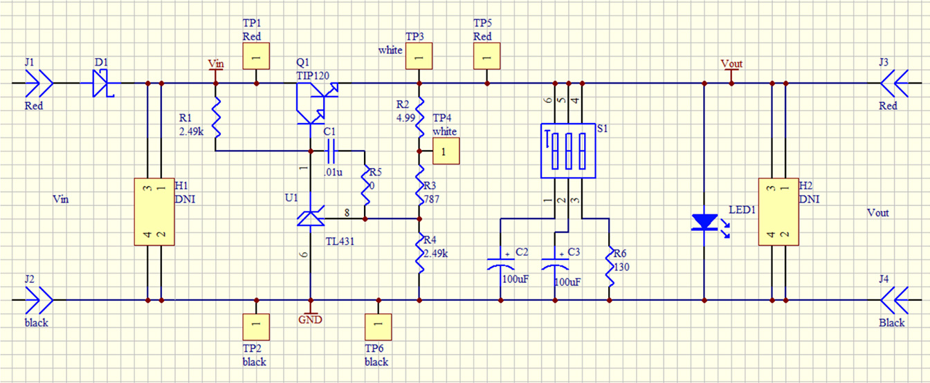
Figure 1: VRTS1.5 schematic
 |
 |
|
Figure 1: VRTS1.5 schematic |
Figure 1: VRTS1.5 schematic 1: Input power +8v |
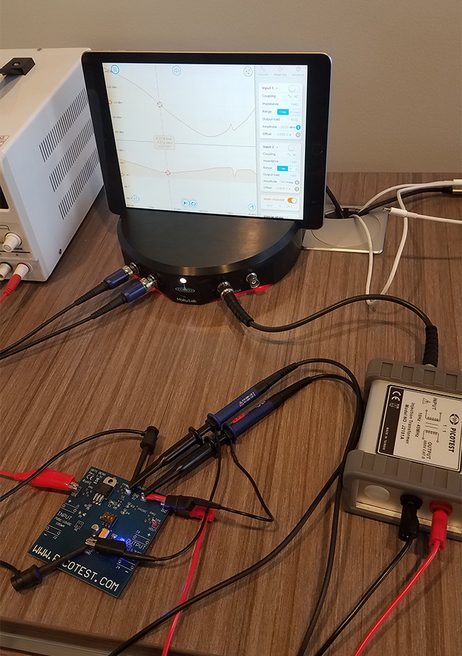
Figure 2 shows the test setup with Moku:Lab, Picotest transformer and VRTS1.5 evaluation board while figure 3 shows a close up of the connections. Moku:Lab input #2 probe is connected to TP3, while Moku input #1 probe is connected to TP4.
The Moku output #1 is driving the swept sine wave through the injection transformer and then across Rinj. Moku:Lab output #2 is not used.
Since we are interested in the transfer function of the regulator; we use Moku:Lab input #2 and input #1 to measure the signals on either side of the injection resistor.
Moku:Lab incorporates a flexible user interface based on the iPad and we set up the Math channel to provide input 2 / input 1 in order to plot the Bode or transfer function.
Initial plot results
The Moku:Lab Frequency Response Analyzer was configured to sweep 100 Hz to 10 MHz at signal strength of -15dBm. The setup and result is shown in figure 4 and clearly this is far from ideal. There is significant noise throughout the plot, most especially below 1kHz.
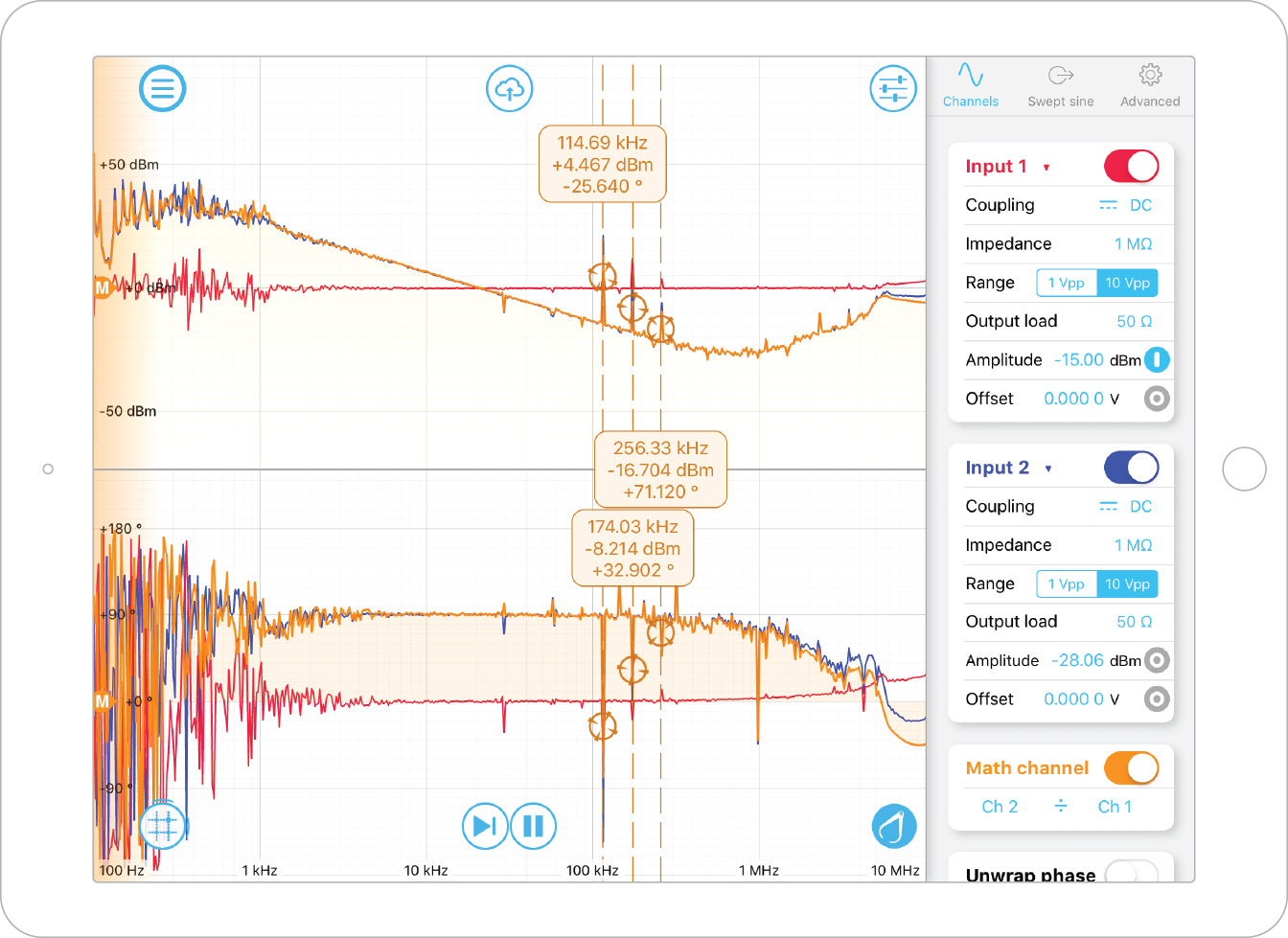
Figure 4: Initial plot
- Math channel (orange) shows transfer function of the control loop.
- Input 1 (red) and Input 2 (blue) shown for completeness.
- The Moku:Lab interface enables quick and easy cursors placement for measurements.
- This plot is not of much use due to the significant noise.
Improved plots
By adjusting the averaging (200ms or 100 cycles minimum) and slightly increasing the settling time (20ms or 20 cycles minimum), we can significantly reduce the impacts of noise in the plots.
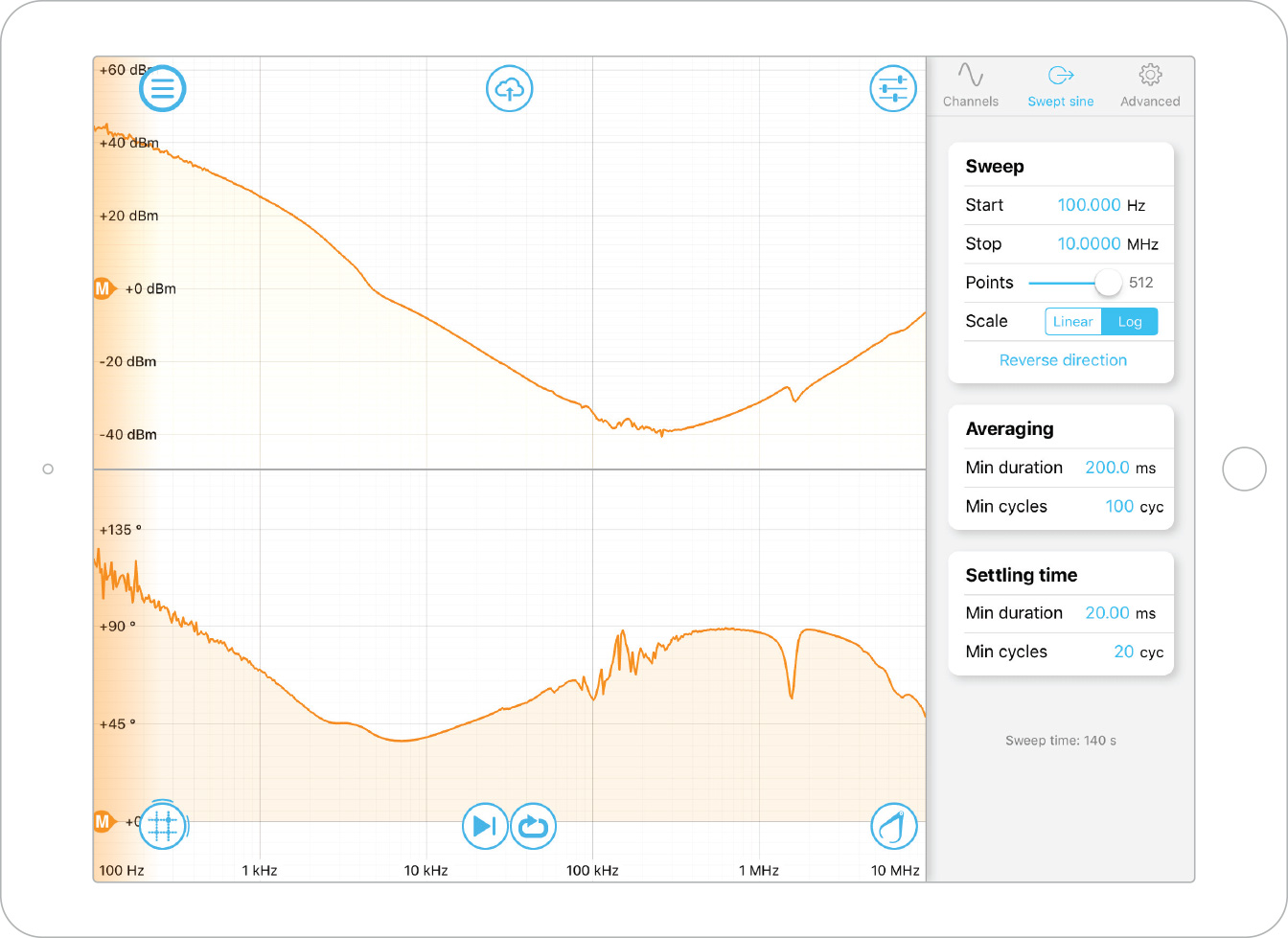
Figure 5: Reduced noise, slightly overdriven
Averaging and settling time configured; this results in a much-reduced noise. It is worth noting the slight non-linearity at the 0dB crossover point. This is likely due to a too large driven swept sine. There is apparent noise on the phase plot in the 100-300 kHz range. We improve this in the next plot by carefully selecting sufficient but not excess.
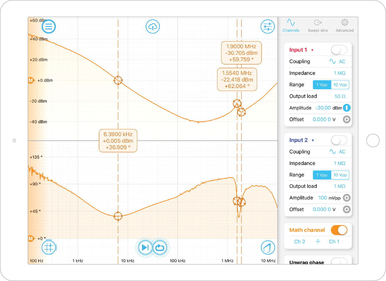
Figure 6: Final Bode plot, tantalum capacitor
In addition to the previously setup averaging and settling times, we now reduced the driven swept sine to -30dBm, using AC coupling use the 1Vpp input range. The 0dB cross over is linear at 6.39kHz and phase margin of 36.9degrees.
Now we want to examine the difference in the regulator response when we change the load capacitor. In the prior plots, we enabled the tantalum 100uF load capacitor via S1-2. Now we enable the electrolytic 100uF capacitor via the S1-1. Figure 7 shows the resulting plot.
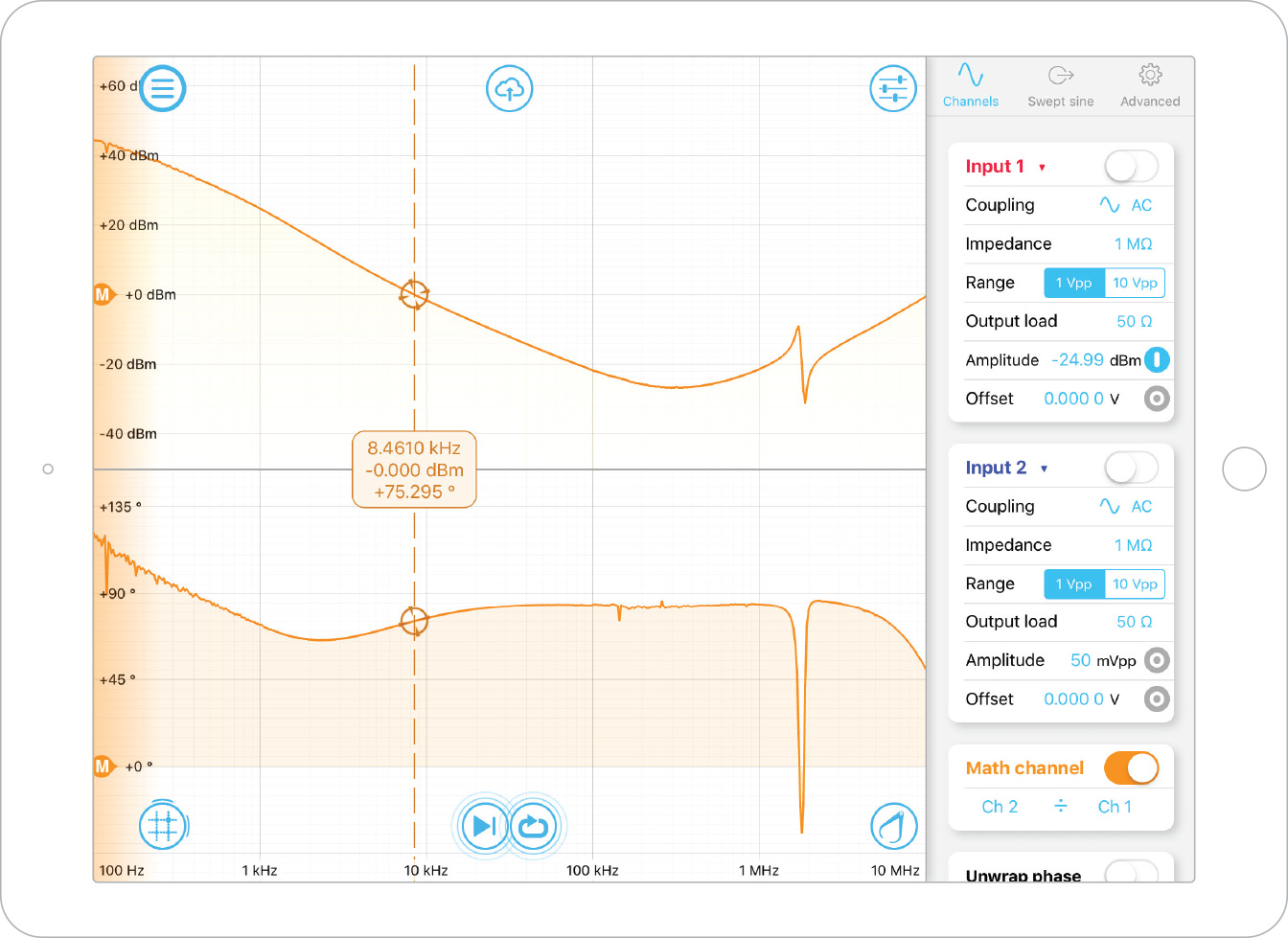
Figure 7: Bode plot with electrolytic load capacitor
The 0dB cross over is linear at 8.461kHz and the phase margin greatly increased to 75.295 degrees.
Summary
In this application note, we have demonstrated the use of the Moku:Lab Frequency Response Analyzer with an injection transformer to examine the frequency response of a linear voltage regulator. Adjustment of swept sine wave output power, together will appropriate sample averaging, resulted in a clear plot of the transfer function, of Bode plot, of the regulator.
Further, we illustrated the difference in phase margin of two different output load capacitors.
The Moku:Lab interface made the instrument setup quick and easy; while the simple sharing of Bode plots (via iCloud screen capture) enabled effective preparation of the graphics used in this document.