
This lab tutorial shows how to use Moku:Go’s Oscilloscope, Spectrum Analyzer, and Programmable Power Supplies along with the TPS63802EVM to confirm important specifications at desired operating conditions. This is useful during development of new products since the Moku:Go can be quickly configured to match expected supply conditions while simultaneously analyzing output characteristics to ensure the module under test will work in your system.

Moku:Go
 Moku:Go combines 15+ lab instruments in one high performance device, with 2 analog inputs, 2 analog outputs, 16 digital I/O pins and optional integrated power supplies.
Introduction
Switch-mode converters are very common electronic systems that are implemented in a variety of ways, so having a set of standard measurements to evaluate the quality of a converter is important for designers who need to decide what type of converter is best for their application. Moku:Go is an ideal test and measurement device for power electronic designers because it integrates various instruments into a single environment that allows for rapid circuit development, testing, and validation.
Datasheets are helpful when deciding between similar types of converters, however, the desired operating conditions may not always be shown in these datasheet charts. This is where Evaluation Modules (EVMs) are helpful and can be easily used alongside the Moku:Go for circuit characterization. It is important to compare key measurements like efficiency and load regulation to datasheet graphs first to ensure the EVM is working properly. That is the goal of this application, to show how you can quickly setup the Moku:Go, a DC-DC converter EVM, and an electronic DC load to confirm common converter characteristics.
Experimental Setup
Components
- Moku:Go (M2 model)
- TPS63802EVM
- Korad Electronic Load
The goal of this lab tutorial is to confirm key specs of the TPS63802 buck-boost converter using Moku:Go as the oscilloscope, power supply, and spectrum analyzer. Below are steps on how to setup the EVM board with Moku:Go and an electronic DC load.
EVM Setup with Electronic Load and Moku:Go
First, connect Moku:Go’s PPSU3 (5 V/1 A) supply to the EVM’s Vin and GND pins at J1 and connect the EVM’s Vout and GND pin at J2 to the DC load. I have set the DC load to its constant resistance (CR) mode where Rload = 10 Ω for now.

Figure 1: Full Moku:Go test setup
There are a few different operating modes on this EVM, so to start JP1 is set to PWM/PFM (Pulse Width Modulation / Pulse Frequency Modulation) mode and JP3 to sense Vout. The EVM is set to have a constant 3.3 V output due to the chosen R1 and R2 values on the PCB.
Next, set Moku:Go’s power supply to 4 V and 1 A limits for now.

Figure 2: Moku:Go PPSU setup
Finally, to enable the board, adjust the shorting jumper at JP2 to the ON position.
To confirm the EVM is operational, look at the Moku:Go’s power supply monitor and the DC load’s monitor as well to see how close we are to the expected 3.3 V using the given test conditions.


Figure 3: PPSU and load setup
Test Procedure
Converter Efficiency
Efficiency measurements can be rather tedious, especially without access to a 4-channel scope that allows monitoring of the input and output power simultaneously. Moku:Go offers a 2-channel solution to this issue since its Oscilloscope features a built-in voltage and current monitor for the power supplies which can be used alongside its two BNC inputs for quick efficiency measurements. There is also the option to automate this measurement through the MATLAB or Python APIs that can read both the power supply sensor data and the voltage input data from Moku:Go’s analog front end. The manual efficiency measurement will be covered here.
Typical efficiency measurements in undergraduate labs are done manually through a table like the one below where the Pin and Pout data are recorded over a varying output current. Taking these measurements are made easier using the math channel in Moku:Go’s Oscillscope due to the function editor feature that allows direct equation input using the two channels as input variables ‘A’ and ‘B’. Type in the output power equation using the shunt resistance directly into the software using the equation editor, in this case Rshunt = 0.5 Ω.

Figure 4: Oscilloscope setup for efficiency measurement
Table 1: Efficiency over varying load and Vin

By plotting Table 1 in Excel and comparing to the TPS63802 efficiency graph from TI’s datasheet, these results are accurate within 4-5%. The losses can be attributed to the long cable lines being used in this test with the Moku:Go and DC load. It is interesting to note that this buck-boost regulator has varying efficiencies depending on its mode of operation over different output current. Buck-boost mode (Vin = 3.3 V) has the best average efficiency across the output current range, while Buck mode (Vin = 5.0 V) and Boost mode (Vin = 3.0 V) have better efficiency at higher currents and lower currents respectively.


Figure 5: Efficiency graph comparison using manual entry
Load Regulation and Load Transient Response
Another important measure of quality of a switching regulator is its ability to maintain a constant output voltage despite changes to the output current, known as load regulation:

where Vnl is the voltage at no load conditions, and Vfl is the voltage at full load conditions. Since this lab is comparing specifications directly to the datasheet, it is important to use the same test parameters for the load regulation which is Vin = 5 V, Vout = 3.3 V, and Iout from 100 mA (no load) to 1 A (full load). By first looking at the load transient graph in Figure 6 below, the output ripple between no load and full load conditions varies greatly. Taking the mean of the output ripple will give us an accurate Vfl and Vnl, however it is best to take each of these measurements individually. This also allows comparison of expected output ripple frequency from TI’s datasheet to the actual ripple frequency being measured on the Moku:Go since this ripple frequency is related to the switching frequency of the PWM or PFM modes.
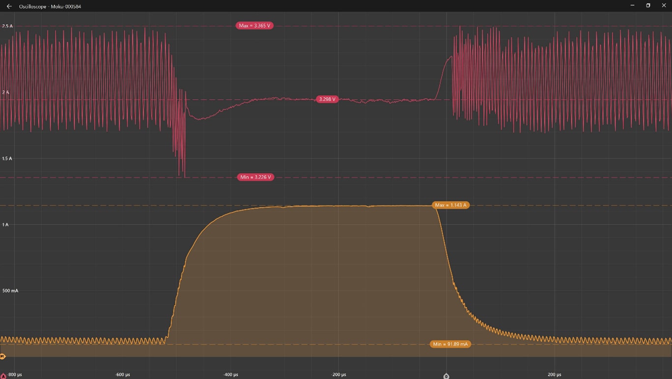
Figure 6: TPS63802 load transient response measured by Moku:Go

Figure 7: TPS63802 load transient response from TI datasheet
The load transient response graphs are fairly similar, with both showing significant ripple during light load operation, and then a much-improved output ripple at full load. This is due to the PWM/PFM feature of the TPS63802 where PFM mode is enabled during light loads to improve efficiency. To ensure the load regulation measurement is accurate, a closer look at the output voltage waveform during PWM and PFM mode is necessary.
Figure 8 below shows the output ripple voltage during light load (Iout = 100 mA) where PFM mode is enabled.

Figure 8: Output ripple voltage in PFM mode
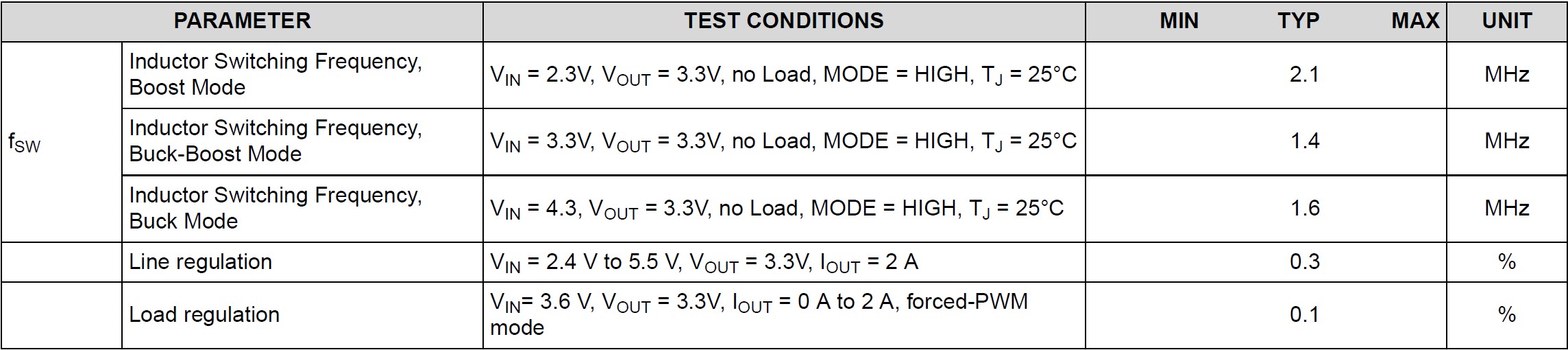
The Vpp of this ripple is quite large at 110 mV, however the mean of this output is very close to the expected 3.3 V where Vnl = 3.313 V. Also important to note is the 135 kHz ripple frequency, which matches the TPS63802 datasheet for switching frequency during PFM operation at low load.

Figure 9: Typical inductor burst frequency vs output current (PFM)
Next is to look at the output ripple at full load (Iout = 1 A) with PWM mode enabled in Figure 10 below.

Figure 10: Output ripple voltage in PWM mode
Here the mean is almost exactly at the expected 3.3 V, with Vfl = 3.296 V, and our ripple is significantly reduced to just 17 mV during PWM operation. The ripple frequency is about 1.8 MHz, also matching with the TPS63802 datasheet expected switching frequency.
Table 2: Typical PWM switching frequency (buck mode)
Using the mean values from Figures 8 and 10 results in a load regulation of:

which again matches the expected load regulation during buck mode (low) with PWM/PFM mode enabled.

Figure 11: Load regulation (PFM/PWM)
The last interesting thing to note about this load transient graph is when looking at the output voltage waveform during the transient period, shown below in Figure 12.

Figure 12: PFM to PWM mode transient response
Due to Moku:Go’s 30 MHz bandwidth and 125 MSa/s sampling rate, it is easy to see how long it takes for the TPS63802 module to react to the change in output current and enable PWM mode. Using the on-screen cursors, where the load transient begins is set as the reference and then another cursor is placed at the peak of when PWM mode is enabled. Figure 13 shows that it takes about 39 µs for the module to change from PFM to PWM mode once the current has increased over the 100 mA threshold.
THD Comparison of PWM and PFM switching modes
Now, switch over to the Spectrum Analyzer instrument and take a look at the quality of the TPS63802’s output in the frequency domain. Moku:Go’s Spectrum Analyzer features a hybrid super-heterodyne FFT that ensure maximum resolution bandwidth (RBW) and sampling rate even at higher frequencies.
A standard measurement of voltage waveform quality is Total Harmonic Distortion (THD) defined as:

where V2n,rms is the RMS voltage of the nth harmonic and Vfund,rms is the RMS voltage of the fundamental frequency. Moku:Go allows an extremely easy way of obtaining this measurement due to its user-adjustable RBW and peak tracking smart cursors.
The test setup for this measurement is Vin = 4.2 V, Vout = 3.3 V, and Iout = 100 mA with one scope probe connected to the output voltage sensor node. At this low current, the converter will be operating in buck mode with PFM enabled. Figure 14 below shows the peak tracking cursors enabled with an adjusted 2.5 kHz RBW at a 1 MHz span. The y-axis has been changed from the typical dBm units to Vrms for quicker calculations.

Figure 13: THD measurement up to 5th harmonic, THD = 5.2%
The fundamental voltage Vfund,rms = 4.750 V, which gives a THD of 5.2% when the converter is operating in its buck mode. Also present are harmonics every 125 kHz, which matches with the ripple we saw during the load transient test during PFM mode.
Now change Iout to be 500 mA, which would enable PWM mode, and see how the THD changes.

Figure 14: THD measurement up to 4th harmonic, THD = 5.1%
The THD of the converter’s output has not changed much at all, however the content of the output spectra has changed. We now see a much higher 2nd harmonic peak with subsequent peaks every 250 kHz, showing that the converter is now operating in PWM mode. This is a great exercise to go along with load transients to show that output ripple and magnitude is closely related to the 2nd order harmonic’s magnitude, as well as the harmonic frequency.
Summary
In this application, measurements from Moku:Go and the TPS63802 datasheet using the TPS63802EVM were successfully compared showing that Moku:Go can act as both an Oscilloscope and Programmable Power Supply to quickly characterize a buck-boost converter under various operating conditions. Using the integrated programmable power supplies and the Oscilloscope together, we were able to quickly change operating conditions of the EVM and obtain detailed output graphs and data to confirm efficiency and load regulation measurements. This allows designers to rapidly test and validate potential ICs for their application, or characterize their own designs using the software-defined instrumentation of Moku:Go.
Have questions or want a printable version?
Please contact us at support@liquidinstruments.com