DC/DC buck converter design and measurement
1 Introduction
DC-to-DC power converters are one of the most common electronic systems implemented today. We commonly see subsystems of this nature in everything from our mobile phone chargers to power supplies in passenger aircraft. Being able to quickly debug and evaluate the quality of various electrical sub-systems is an extremely important skill for an Electrical engineer. The United States Air Force is specifically interested in applications of power conversion, as many of our systems employ a variety of power electronics subsystems throughout.
What is a buck converter?
A buck converter is a type of switching step-down converter. It is a commonly used sub-system to efficiently reduce the voltage from an input source (supply) to an appropriate level for the output (load). Buck converters arc a type of switching converter where a transistor will be used to act as a switch, and either isolate or connect the supply side of the of the circuit to the load. A key advantage to the buck converter is the efficiency of the voltage conversion. Typically we can expect 90% or greater efficiency from a well designed buck converter.
Objectives: This lab will aim to:
- Introduce the basic theory behind the buck converter
- Identify sizing considerations for the individual components
- Demonstrate analysis and measurement techniques for an actual implementation
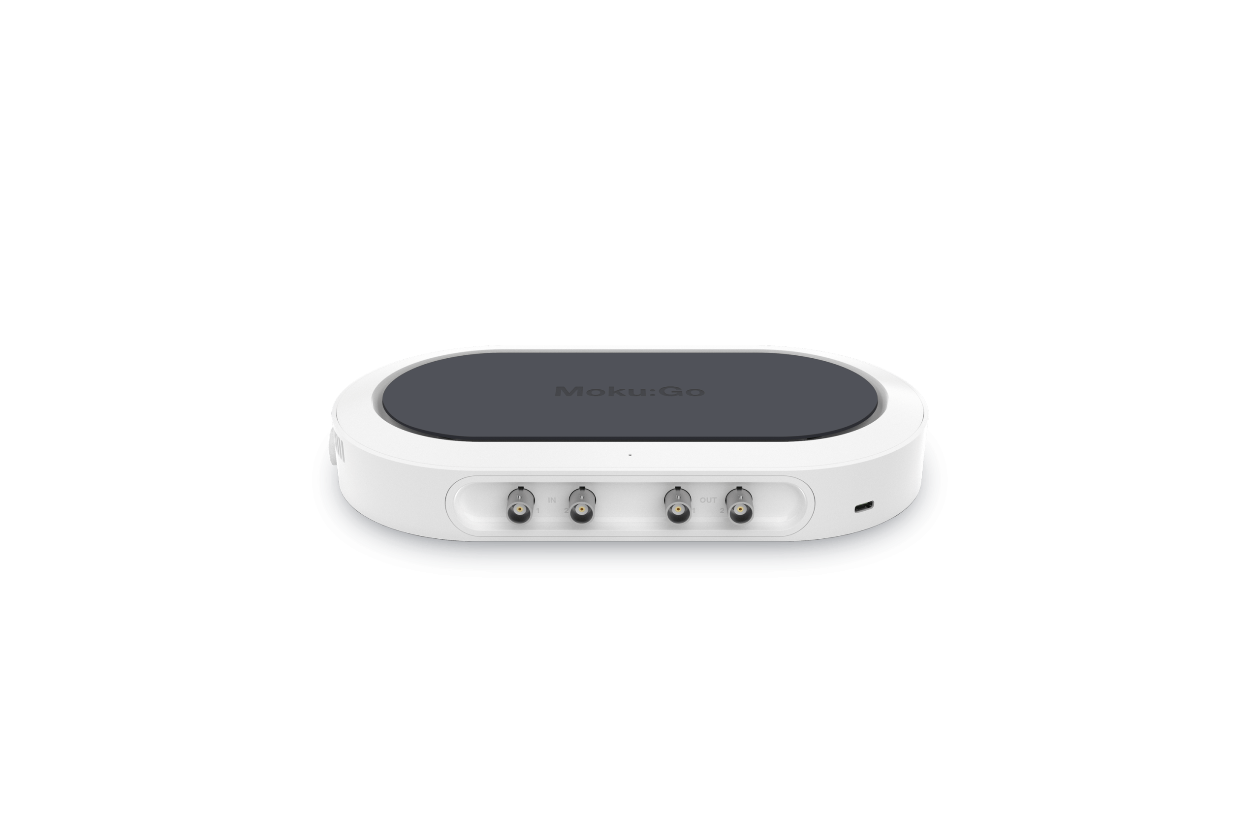
The laboratory portion in this write-up will be based on Moku:Go by Liquid Instruments. A variety of oscilloscopes, DC power supplies, and function generators will suffice for this laboratory. The Moku:Go was chosen for this lab experiment, as it contains all required test equipment for this laboratory in a single device.
The overall goal of this effort was to start developing a series of comprehensive laboratory experiments that could either be conducted as stand-alone exercises or coupled with in-depth theory. The aim is to expose students to a variety of key concepts and allow them to simultaneously explore their practical applications. The labs are intended to provide a cursory exposure to the theory and necessary calculations, but will not provide all necessary derivations commonly found in most Electrical Engineering text books. This strategy was chosen to present a more approachable lab to a wider variety of student levels of expertise, with the awareness that the labs could readily be coupled with increased theoretical discussion.
2 Materials
The following bill of materials are required to fully execute the laboratory portion of this tutorial.
2.1 Test Equipment
- 1x Moku:Go OR
- 1x function generator capable of generating a 50 kHz PWM signal
- 1x oscilloscope
- 1x power supply capable of 12 V and 150 mA
- 1x proto-board or modular Printed Circuit Board (PCB) design described below
2.2 Electronics Components
- 1x 470 µH inductor (652-2100LL-471-H-RC or similar)
- 1x P-Channel MOSFET (IRF9Z24NPBF or similar)
- 1x N-Channel Transistor (2N3903 or similar)
- 1x 1000 3-watt resistor (W3M1000J or similar)
- 4x 1 kΩ ¼ watt resistors
- 1x 330 Ω ¼ watt resistors
- 2x 100 µF capacitors (80-ESK107M050AG3AA or similar)
- 1x Schottkey diode (MBR745G or similar)
3 Theory
Switching converters are an efficient class of circuits used to convert an input DC voltage to a different output DC voltage. In this laboratory we will specifically consider a buck converter that is theoretically designed to drop a DC input voltage to any output level less than the input. In practice, the maximum output will be slightly less than the input voltage due to losses in the various electrical components. In a future lab, we will explore the boost converter which can allow for outputs greater than the input.
3.1 Basic Switching Converter
The basic switching converter in Figure 1 will use a Pulse Width Modulated (PWM) input signal to drive a transistor that acts as a switch. The voltage across the load will then alternate between Vs and 0 V when the PWM signal is high and low respectively. From this it should be fairly intuitive that the average voltage across the load will increase as a function of increasing or decreasing duty cycle on the PWM input signal.
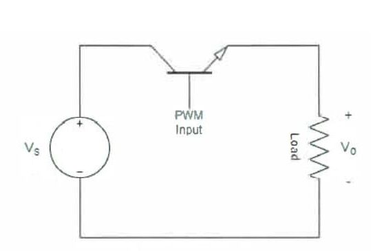
Figure 1: Basic switching converter
For a pulsed input with duty cycle (D) into this circuit, a pulsed output as shown in Figure 2 will result. For this ideal simple circuit design, the pulsed output duty cycle will exactly match the input PWM duty cycle where:

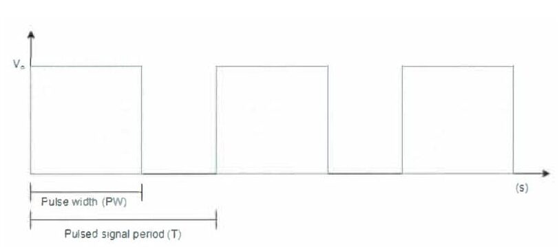
Figure 2: Output voltage (V0) as a function of switched input duty cycle
From Figure 1 and 2 we can deduce that the average voltage across the load will be described by:

and the average output is directly correlated with the duty cycle. In many applications, a pure DC output will be desired.
3.2 Ideal Buck Converter
In order to generate a purely DC output at the load, a low-pass filter can be applied to the basic switching converter as shown in Figure 3. If we could generate an ideal low-pass filter, the output measured across V would naturally become Vs (D) as indicated above. However, since we know we cannot create an ideal low-pass filter, the following theory will introduce sizing considerations for the inductor and capacitor based primarily on the load and PWM input frequency.
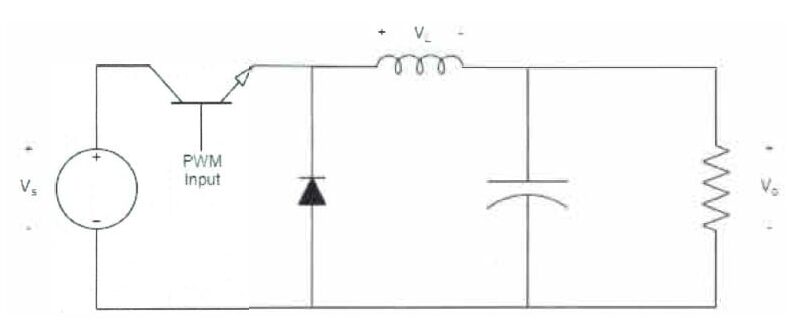
Figure 3: Basic DC to DC buck converter
The following analysis assumes that the diode in Figure 3 will remain forward biased at all times. As such, we need to ensure that the inductor current remains positive, or in other words in a continuous current region of operation. If the inductor current is permitted to return to zero during each period of the PWM input signal, the inductor would be operating in a discontinuous current region, and the following analysis will break down. Essentially in the discontinuous current region you would no longer see the close correlation between PWM input PW and output voltage at the load, V0. In order to size the inductor appropriately, we can use the following equation:

where f is the PWM input frequency, Prat is the maximum power rating for the converter and k is the ratio of maximum to minimum output power output you wish to design for. This equation will help us find the minimal value for the inductor Lmin given that we hold f constant. Given that many loads may have various power draws, Lmin should be sized by tuning k and f. We will typically design such that k is between 3 and 10, and many power electronics applications will keep f around 50 kHz or less. However, it is not uncommon to see switching frequencies in the 100 kHz range at this point. In cases where a single converter may be needed for various applications, we must account for the balance of each parameter in equation 3. The capacitor in Figure 3 will control the ripple voltage across the load. The ripple voltage is the minor variation in voltage across the load caused by the constant charging and discharging of the capacitor as the PWM input switches on and off respectively. Acceptable levels of ripple voltage are another design consideration that must be planned for in the design of the buck converter. Equation 4 allows for the calculation of the minimum capacitance level if we know the desired maximum level of ripple voltage (ΔV0-pp)

3.3 Example Configuration
Let us assume we have the following configuration:
- Vs = 12 V
- RL = 100 Ohms
- f = 50 kHz
- Pmax = 1.44 W
- Pmin = 0.36 W
- Ripple Voltage <= 3 mV
If we wanted to assure that we could maintain continuous current down to 6 V, we could assume D to be 50%. In actuality D may differ slightly based on sizing of the individual components, but 50% is a good starting point.

Notice that we could increase our PWM frequency if we wanted to further reduce the required inductance, up to the maximum switching frequency of the transistors. For instance, if we know we have 470 µH inductors available, we could now go in and find the required switching frequency to make the scenario above work. In this subsequent case, we would need a switching frequency of 53.191 kHz to ensure continuous current while dropping the voltage across the load to 6 V.

We can now size our capacitor to account for the desired ripple voltage at the output.
3.4 Switch Design
The left half of the circuit in Figure 3 was an over simplification of reality. In order to properly account for various voltage levels at the input and differing levels between the PWM input and the source voltage, an increase in complexity is warranted.

Figure 4: Full DC to DC buck converter
As you can see in Figure 4, the right half of the circuit is identical to Figure 3 above. However, the left side of the circuit incorporates the necessary logic to allow an external input to properly enable the switching without causing damage to any of the components. This switch design would be effective for most switching type DC-to-DC converters. We have essentially created a high-side switch using the P-Channel MOSFET. We use an NPN Transistor to provide the required gate input to the MOSFET and drive the gate on the Transistor with our PWM input. This PWM input could come from most any function generator capable of frequencies near 50 kHz. In the next section, we will evaluate the design and test our predictions from above.
4 Simulation
Using Figure 4 above, we will now use both Multisim and LT Spice to simulate and test the effectiveness of our design above. Ultimately our goal is to test the predictions based on theory in simulation before implementation. Additionally, we will investigate the predicted efficiency of this design. In keeping with the focus of using switching type converters, a normal goal would be to achieve efficiencies in the designed range near 90% or greater efficiency. However, we expect that the design will lose efficiency in both simulation and in practice as we get closer to the limits on the design of the components. Additionally, based on design we expect that increased switching frequencies will result in a reduction in efficiency, as each switching cycle, there will be a period where the P-Channel MOSFET has both a high voltage and current through it. The duration of this transition will not change with increased frequency. However, the total ratio of time for this transitional period within the P-Channel MOSFET will naturally increase with increased switching frequency. Recall, that the primary reason for using a high switching frequency was to reduce the required inductance value L1.
In order to estimate the efficiency of the design, we merely measured the power across the load, and compared it to the power out of the source. With MultiSim, we were able to probe both points in the circuit very easily. In practice, we will need to measure the current and voltage at each point for comparison.
4.1 Efficiency
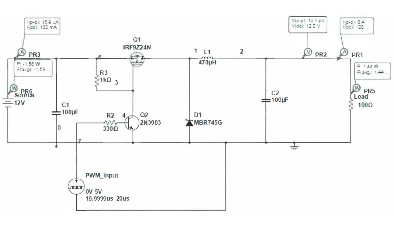
Figure 5: Simulation with 100% duty cycle
The following results were obtained by providing various values for duty cycle from 100% down to 10%. Key observations were that the design of the buck converter resulted in a decreased efficiency as the duty cycle decreased as shown below.
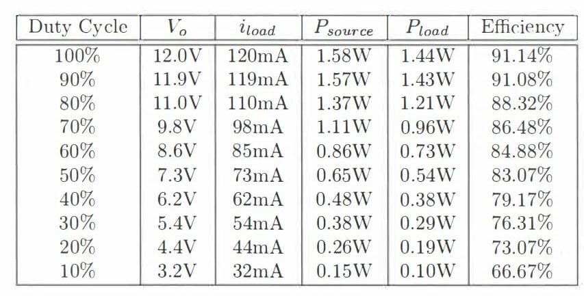
Table 1: Simulation results
4.2 Experiment Design Goals
With the baseline results established in the previous table, our goal with this effort was to design a configurable Printed Circuit Board (PCB) that would allow a student to test a variety of hypothesis based on a baseline knowledge of component relationships. For instance a few interesting hypothesis to test would be:
- Relationship between switching frequency and observed efficiency
- Relationship between inductance and switching frequency
- Relationship between capacitance and ripple voltage
In order to accommodate rapid explorations as indicated above, a configurable PCB where key components Ll, Cl, C2 and load values could all be changed easily. Additionally, we wanted to allow for various techniques to provide feedback and control the duty cycle or source of PWM signal.
4.3 Configurable DC-DC Buck Converter PCB
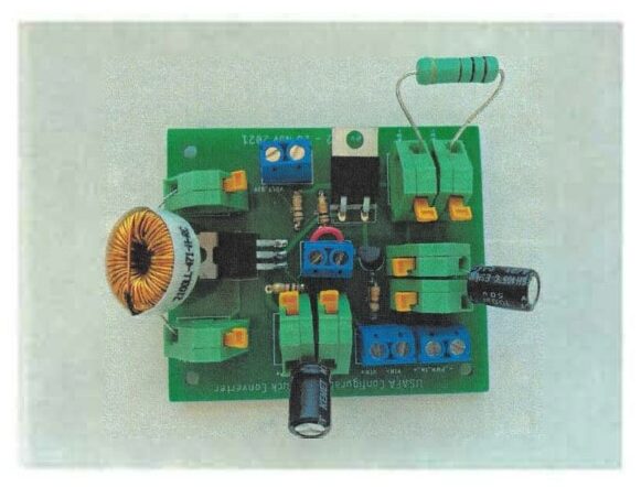
In order to achieve a modular circuit that would allow us to explore the stated design goals the circuit from Figure 4 was designed into the following PCB. Of note, the goal was to realize a simple laboratory aid versus a commercial grade DC-DC buck converter. Rather than permanently affixing any of capacitors, inductor or loads onto the board, simple terminal blocks were used. While this design could easily be built on a basic prototyping board, we chose to design a configurable PCB to aid with quicker investigation of key concepts versus time spent having the student build the prototype. While there is value in the prototyping exercise, that is not the aim of this laboratory experiment.
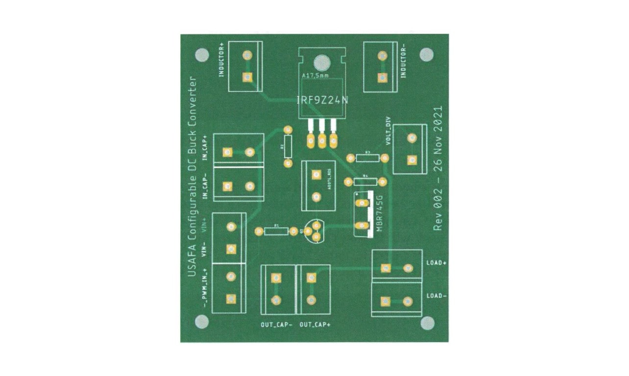
Figure 6: Configurable buck converter PCB
The circled areas in Figure 7 highlight the terminal blocks that can be used to change out values for C1, C2, L1 and the Load from Figure 4.
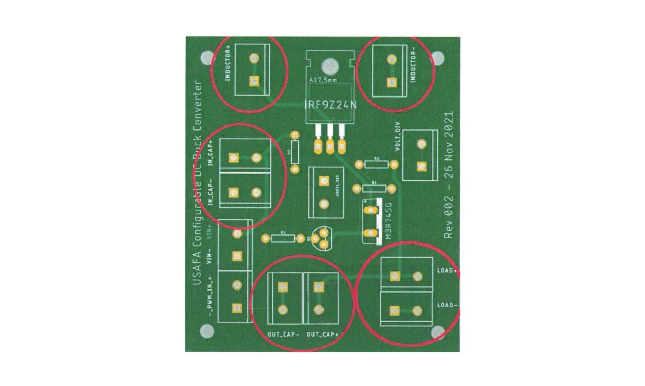
Figure 7: Configurable buck converter PCB – customizable components
The circled areas in Figure 8 show where a PWM signal can be provided to the controller. Under most circumstances the PWM input would be connected to the circled area on the bottom left. However if you are using a chip like the TL-5001 PWM Controller, you need to provide the input in the center circled terminal block. Using the center terminal block will bypass the NPN transistor and provide the signal direct to the P-Channel MOSFET. Additionally, the center terminal block allows for you to connect an additional resistor between the Gate of the P-Channel MOSFET and the collector of the NPN transistor.
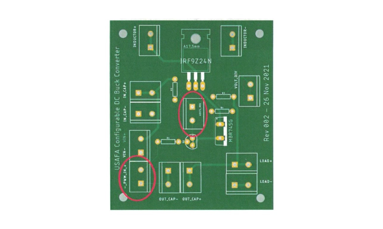
Figure 8: Fully built configurable buck converter
The terminal block circled in Figure 9 provides an output of a voltage divider in parallel with the load. This voltage divider can be custom configured to provide various different voltage levels to incorporate a feedback loop to allow for dynamic control of the duty cycle and output voltage across the load.
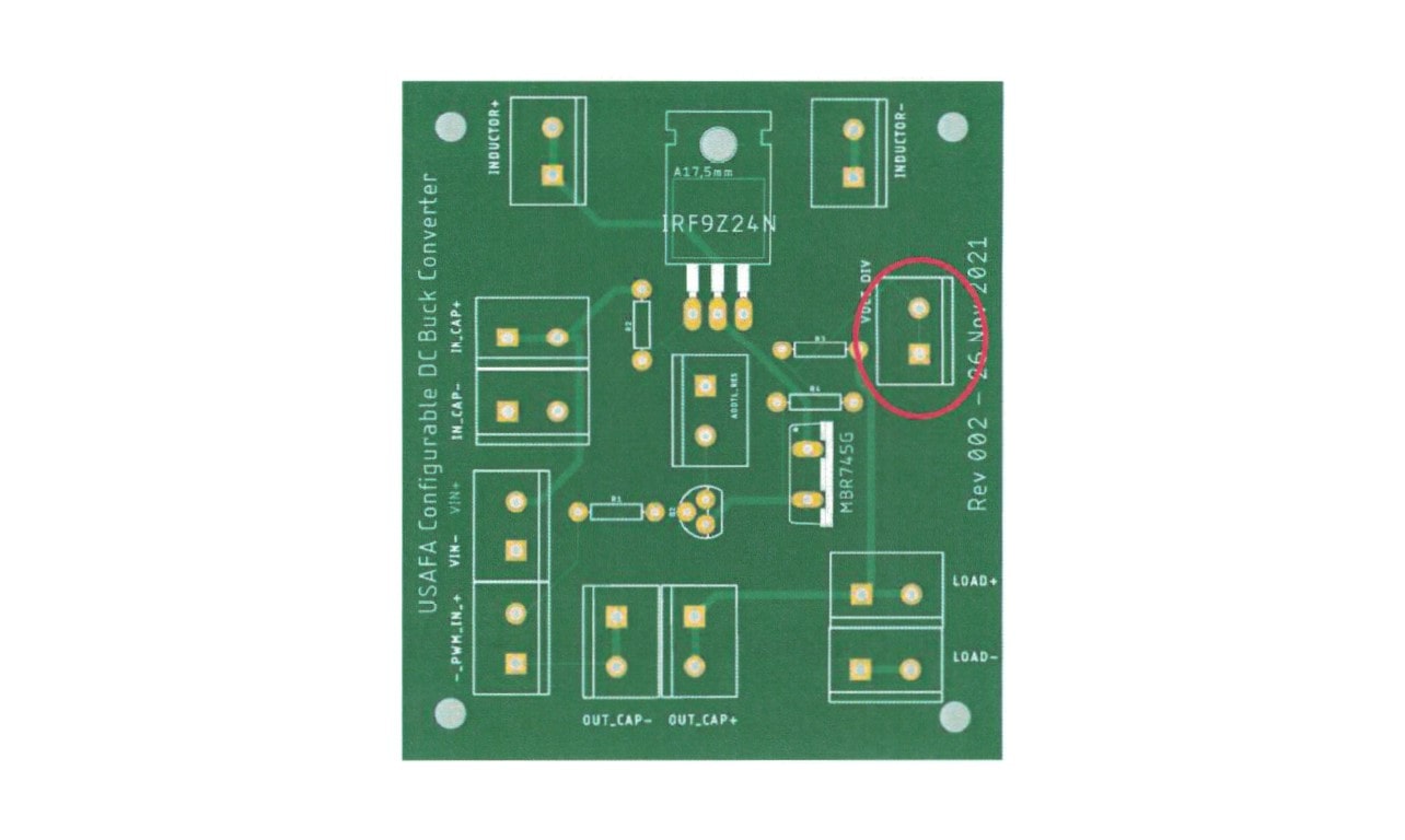
Figure 9: Configurable buck converter PCB – voltage divider for feedback control
Figure 10 shows the fully configured DC-DC buck converter PCB per the design in Figure 4.
Figure 10: Configurable buck converter PCB
5 Experimental Results
5.1 Comparison to Simulation Efficiency
In this section we will compare the performance of our buck converter to the simulation results. As you can see below in Table 2, the efficiency did decrease as expected from simulation, but the overall trends and magnitudes are similar. Additionally, the voltage across the load closely matched our simulation (within 0.2 V at each duty cycle). Clearly we can expect some variation with actual components, but the results below provide some level of basic assurance that our buck converter is working as intended, and is always a great first step before in depth investigation.
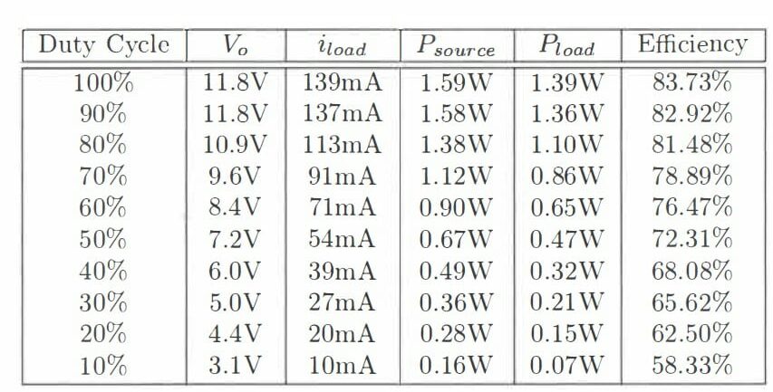
Table 2: Simulation results
5.2 Gate Source Voltage for P-Channel MOSFET
With this basic comparison in place, we can now take some additional measurements to observe the functional regions for chosen components. One interesting measurement is to test the gate-to-source voltage for the P-Channel MOSFET to ensure it is below the maximum value specified in the component data sheet. Per the data sheet, VGS,Max = ±20V. Using the math channel on an oscilloscope and the two input channels, we can measure the voltages at both the gate and the source as seen in Figure 11. As you can see below, even with the overshoots, we never approach the limits for the component.
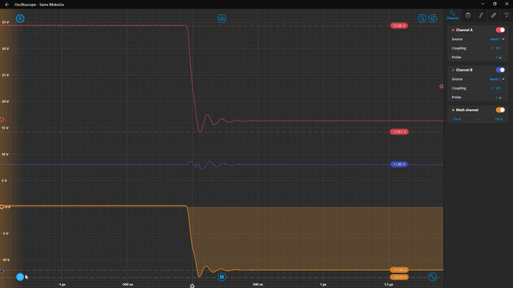
Figure 11: VGS with source input of 12 V
In Figure 11, we plot our P-Channel MOSFET gate voltage on channel A, and the P-Channel MOSFET source voltage on channel B. We then use the math channel to find VGS. Even with the overshoots, we never approach the limits for the component. However when we increase the input source voltage to the buck converter to 16 V as shown in Figure 13, the overshoots are measured at -18.62 V. Therefore, we likely risk damage to the FETs gate at anything above about 17 V.
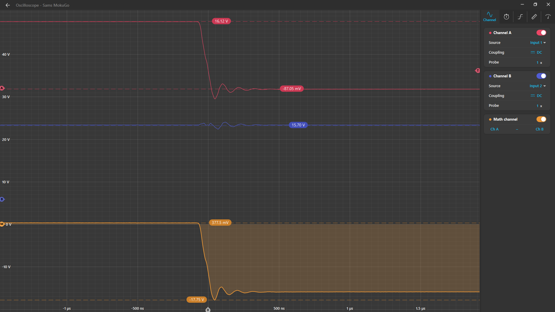
Figure 12: VGS with source input of 16 V
Without moving the oscilloscope input probes, we can make another interesting measurement. We can measure the time from when the PWM signal goes high to when the gate voltage of the P-Channel MOSFET settles to zero. By setting the left most cursor as the reference, we can sec that this time is 1.5 µs. Measurements like this can provide support for upper limits on switching frequency given the chosen components.
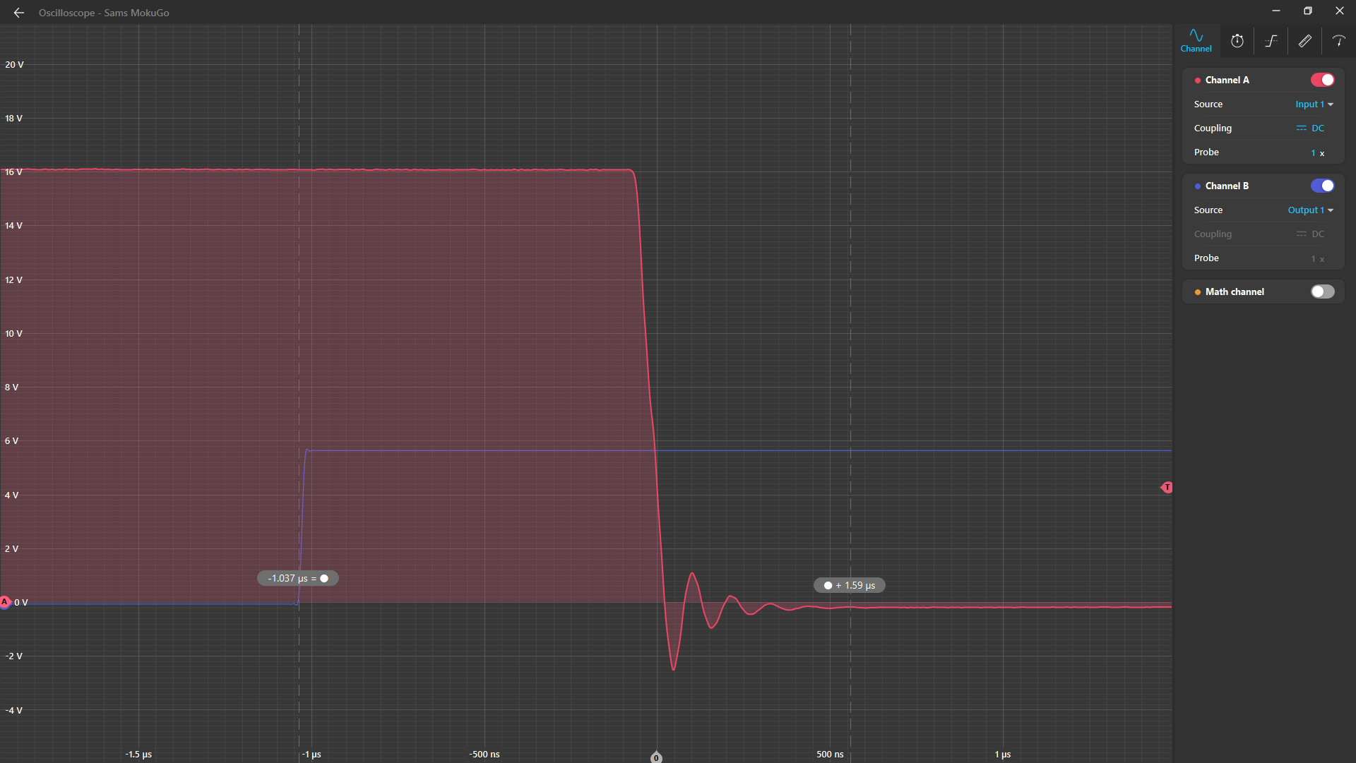
Figure 13: Transition time
5.3 Additional Measurements and Experiments / Future Experiments
The previous demonstrated measurements were merely a small subset of the types of explorations you could make with this board. Clearly we could change out component values to test various hypothesis. Additionally you could create a feedback loop and have students design a PID Controller to maintain a constant voltage output.
6 Summary
All-in-one instrumentation systems like the Moku:Go provide a flexible solution to augment purpose built laboratories, and in many cases can provide enhanced flexibility to bring demos to the students with greater repetition and frequency. When coupled with tailored experiments as discussed above, we may have the opportunity to break certain barriers that currently prevent many students from choosing to study Electrical and Computer Engineering.